Affordable pH meter
Our home vineyard delivers about 1000 liters of wine every year. It takes some effort to keep good quality and pleasure for all friends tasting the must, new wine and “senior” wine reserves. One of the most important tasks in wine quality management is controlling the biological and chemical state of the wine. The wine can be monitored in special laboratory or in home lab. Of course home lab become rational when quantity of the wine is high enough to justify expenses in special equipment. There is some low cost equipment available for wine analysis, mostly with titration techniques, but chemical lab equipment is rather expensive and many hobby wineries avoid buying such equipment. I hope this post can contribute a bit to change that. I will describe the development of simple pH meter in detail.


Hardware
I will not go much into the details of the pH measurement principle. The topic is explained elsewhere quite deeply:
Complete instrument has only few building blocks: pH electrode, analog frontend, AD converter, microcontroller, power supply and user interface. These are usual building blocks for many similar applications and I would like to describe the circuit in every detail to help others building similar projects based on this one. First I will describe the hardware part, followed by software description. The circuit block diagram is shown in following image:

pH Meter Block Diagram
The sensor: pH electrode
I didn’t want to experiment with some expensive pH probe, because those sensors are very sensitive devices. The can degrade very quickly when not properly connected. Simple short circuit at the electrode can destroy it or at least requires not so easy process of electrode regeneration. So, when experimenting with the pH electrodes: Be careful!
Great source for such electrodes is eBay. Just search for “pH Electrode BNC”.
Analog frontend (AFE)
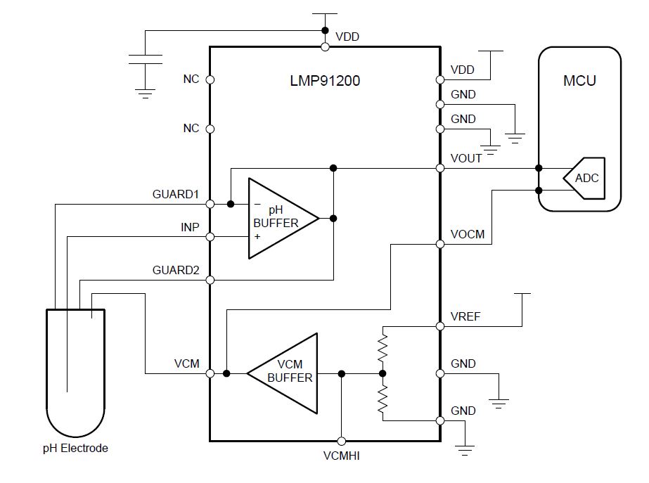
The pH meter is based on TI’s LMP91200 sensor analog frontend. The LMP91200 is designed for 2-electrode sensors and provides all of the functionality needed to detect changes based on a delta voltage at the sensor. It works over a wide voltage range of 1.8 V to 5.5V. The most important feature for pH electrodes is LMP91200 extremely low input bias current, which is also true in absence of supply voltage. This will reduce degradation of the pH probe and provide longer electrode life.
LMP91200
The interesting thing about LMP91200 is its development cycle. I had about two year old samples from TI sampling system. The LMP91200 AFE datasheet from year 2012 has all pins describedand defined. New revision of the same datasheet has all pins which are normally not used omitted from the description with only recommended connections to disable all extended functionality. I don’t know if the internal circuit was really changed or they just skipped the functions which were not operating as expected. In any case, here is old datasheet, which is not available anywhere and may be useful as source for undocumented features of the LMP91200. The difference is as follows:
New LPM91200 without pins described

Old LMP91200 with all pins
A/D Converter
I found nice stock of AD7715 in my old component storage. It is a Σ-Δ ADC which I used in past for some sensor projects with great success. It has differential input and internal PGA, both not really needed for this pH meter, but may be useful for other projects based on this one. It has few on-chip control registers allowing adjustment of the PGA gain, ADC configuration, filter cutoff and output update rate. Depending on the PGA gain it can handle unipolar input signal ranges of 0 mV to 20 mV, 0 mV to 80 mV, 0 V to 1.25 V and 0 V to 2.5 V. The part contains self-calibration and system calibration options to eliminate gain and offset errors on the part itself or in the system. The package is “hobby friendly” SO-16-Wide.
The AD converter can be as good as the voltage reference used for the conversion process. I decided to invest a bit more into the voltage reference to avoid accuracy and long term stability issues in future with such instrument. It is a bit overkill for the pH application, because the pH measurement is calibrated as the whole system, but for any other instrumentation applications it can save few gray hairs.
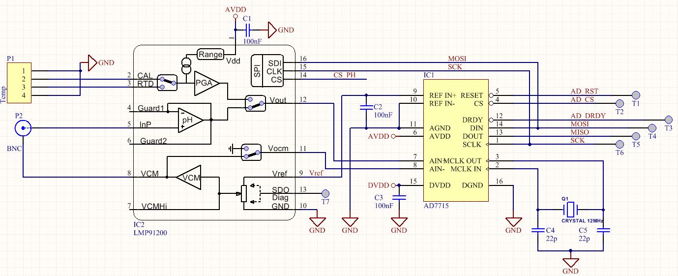
LMP91200 + ADC with 2,5V reference
Microcontroller
Microcontroller for this instrument can be low on resources. Good choice is the one with good development support. Combination of low cost and excellent development environment is the STM32F0 from ST with free Keil MDK edition for STM32F0/L0. The price is below 1 EUR and the plastic housing is also “hobby friendly” – TSSOP20. It has USB interface, which can be used instead of user interface to connect with tablet, mobile phone or PC. In presented project, we are dealing with conventional user interface: alphanumeric LCD and rotary encoder.

Microcontroller, encoder and 2×16 LCD
User interface
The most common user interface for simple microcontroller projects can be alphanumeric LCD and simple rotary encoder. Both can provide simple and efficient control over the instrument features, calibration, settings, etc… The connection diagram is shown above.
Now it’s time to solder everything together and start programming.
Software
Software development is based on free Keil MDK Version 5, the MDK for STM32F0 and STM32L0 edition, which includes the ARM C/C++ Compiler, the CMSIS-RTOS RTX Kernel, and the µVision IDE/Debugge free of charge. The source code is Unlicensed.
AD7715
Functional block diagram of the AD7715 reveals requirement for SPI interface. We will not use DRDY signal. It can be polled from the status bit in the internal register of the AD7715.
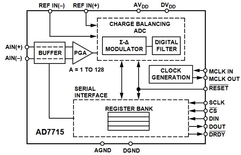
AD7715 Functional block diagram
AD7715 is connected to Cortex M0 via four pins: MISO, MOSI, SCK and CS. It is also possible to use shared MISO/MOSI. I decided to prepare the driver with bit-banging serial interface, which can be ported to any other microcontroller without hardware SPI interface. The communication is very simple and can be implemented on smallest MCUs. Here is description for the STM32F0.
First we have to define pins for communication. In our case, the pinout is CLK: PA5, MOSI: PA7, MISO: PA6 and CS: PF1:
/* CLK: PA5 */ #define AD7715_CLKPORT GPIOA #define AD7715_CLKPINn 5 /* MOSI: PA7 */ #define AD7715_MOSIPORT GPIOA #define AD7715_MOSIPINn 7 /* MISO: PA6 */ #define AD7715_MISOPORT GPIOA #define AD7715_MISOPINn 6 /* CS: PF1 */ #define AD7715_CSPORT GPIOF #define AD7715_CSPINn 1 |
Now define the bit masks for the pins:
#define AD7715_MOSIPIN ((uint16_t)(1U<<AD7715_MOSIPINn)) #define AD7715_MISOPIN ((uint16_t)(1U<<AD7715_MISOPINn)) #define AD7715_CSPIN ((uint16_t)(1U<<AD7715_CSPINn)) #define AD7715_CLKPIN ((uint16_t)(1U<<AD7715_CLKPINn)) |
When pinout is defined, it’s time to init the pins. The internal register banks and hardware blocks must be connected to clock source first in order to operate properly, including programming the registers. Our pins are connected to GPIOA ind GPIOF blocks. They are both on AHB bus. The AHB peripheral clock enable register is within RCC, the Reset and clock control block. The register definitions and bit masks for accessing bits within the registers are all defined in the device include file. Our microcontroller is STM32F070C6, the 20 pin “small beast” has all the peripheral register’s definitions, bits definitions and memory mapping in file stm32f070x6.h.
GPIO Clock enable

AHB peripheral clock enable register (RCC_AHBENR)
RCC->AHBENR |= RCC_AHBENR_GPIOAEN; /* Enable GPIOA clock */ RCC->AHBENR |= RCC_AHBENR_GPIOFEN; /* Enable GPIOF clock */ |
GPIO Output configuration
Basic structure of the IO pin is shown in the following figure:
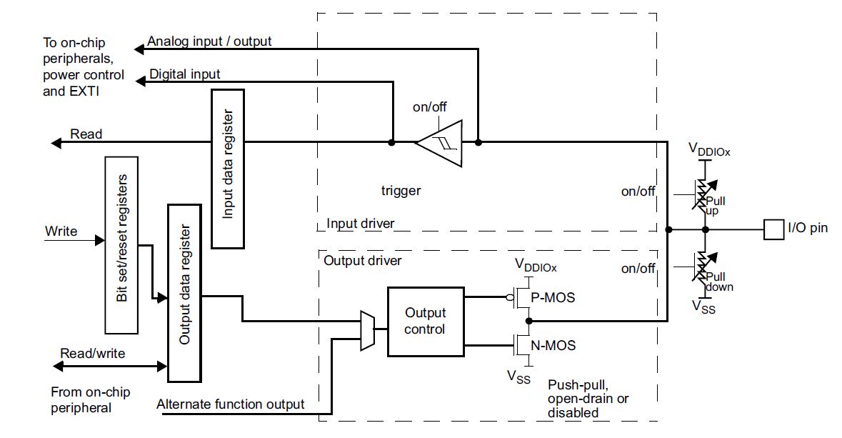
Basic structure of an I/O port bit
For each GPIO pin we have to define 4 different configurations: pin mode, output type, speed and pullup/down with the registers MODER, OTYPER, OSPEEDR and PUPDR, respectively. The pins MOSI, CLK and CS will be Medium speed, Push-Pull outputs without pullup/down. Each of 16 GPIO pinse per port has two bits in each of the 32-bit MODER, OSPEEDR and PUPDR registers. The access to the bits is therefore double pin number, e.g. for PA10, the bit fields in the GPIOA->MODER register are 10*2: bits 20 and 21. The register OTYPER configure the I/O output type.
Each two bits per port in MODER register can configure corresponding port to following four possible configurations:
00: Input mode (reset state)
01: General purpose output mode
10: Alternate function mode
11: Analog mode
The bits written in OTYPER configure the I/O output type:
0: Output push-pull (reset state)
1: Output open-drain
Three possible speed configurations cen be selected by writing the bits to OSPEEDR:
x0: Low speed
01: Medium speed
11: High speed
And finally, the bits are written to PUPDR to configure the I/O pull-up or pull-down:
00: No pull-up, pull-down
01: Pull-up
10: Pull-down
11: Reserved
In our case, we need medium speed, no pullop/down, pushpull output. With the help by the port definitions above we can initialize port pins as follows:
/* CLK push-pull, no pullup */ AD7715_CLKPORT->MODER &= ~(3ul << 2*AD7715_CLKPINn); AD7715_CLKPORT->MODER |= (1ul << 2*AD7715_CLKPINn); AD7715_CLKPORT->OTYPER &= ~(1ul << AD7715_CLKPINn); AD7715_CLKPORT->OSPEEDR &= ~(3ul << 2*AD7715_CLKPINn); AD7715_CLKPORT->OSPEEDR |= (1ul << 2*AD7715_CLKPINn); AD7715_CLKPORT->PUPDR &= ~(3ul << 2*AD7715_CLKPINn); /* MOSI push-pull, no pullup */ AD7715_MOSIPORT->MODER &= ~(3ul << 2*AD7715_MOSIPINn); AD7715_MOSIPORT->MODER |= (1ul << 2*AD7715_MOSIPINn); AD7715_MOSIPORT->OTYPER &= ~(1ul << AD7715_MOSIPINn); AD7715_MOSIPORT->OSPEEDR &= ~(3ul << 2*AD7715_MOSIPINn); AD7715_MOSIPORT->OSPEEDR |= (1ul << 2*AD7715_MOSIPINn); AD7715_MOSIPORT->PUPDR &= ~(3ul << 2*AD7715_MOSIPINn); /* CS push-pull, no pullup */ AD7715_CSPORT->MODER &= ~(3ul << 2*AD7715_CSPINn); AD7715_CSPORT->MODER |= (1ul << 2*AD7715_CSPINn); AD7715_CSPORT->OTYPER &= ~(1ul << AD7715_CSPINn); AD7715_CSPORT->OSPEEDR &= ~(3ul << 2*AD7715_CSPINn); AD7715_CSPORT->OSPEEDR |= (1ul << 2*AD7715_CSPINn); AD7715_CSPORT->PUPDR &= ~(3ul << 2*AD7715_CSPINn); |
GPIO Input configuration
Similar to above outputs, now we can configure pin MISO as input with the pullup:
/* MISO Input, pullup */ AD7715_MISOPORT->MODER &= ~(3ul << 2*AD7715_MISOPINn); AD7715_MISOPORT->OSPEEDR &= ~(3ul << 2*AD7715_MISOPINn); AD7715_MISOPORT->OSPEEDR |= (1ul << 2*AD7715_MISOPINn); AD7715_MISOPORT->PUPDR &= ~(3ul << 2*AD7715_MISOPINn); AD7715_MISOPORT->PUPDR |= (1ul << 2*AD7715_MISOPINn); |
Write and read GPIO Pins
Output pins are set or reset by writing to GPIO port bit set/reset register. Lower 16 bits are used to set, upper 16 bit are for reset the output pins. The operation can be done by accessing the single register and shifting the bits 16 places when we want to set the pins to 0. The procedure for set or reset the MOSI line is then:
void AD7715_SetMOSI(int state) { if (state) AD7715_MOSIPORT->BSRR = AD7715_MOSIPIN; else AD7715_MOSIPORT->BSRR = AD7715_MOSIPIN << 16; } |
and similar for CS and CLK. The content of the output state can be read or set by accessing the GPIO port output data register. When pin is configured as input, the state of the pin is reflected in GPIO port input data register. The state of the MISO pin can be read with the following function:
uint8_t AD7715_ReadMISO(void) { uint8_t rv = 0; if ((AD7715_MISOPORT->IDR & (AD7715_MISOPIN)) != 0) { rv = 1; } return rv; } |
Transfer a byte
The function to simultaneously transmit and receive a byte on the AD7715 with such “software defined SPI” is shown below. It returns the received byte.
uint8_t AD7715_transferbyte(uint8_t byte_out) { uint8_t byte_in = 0; uint8_t bit; for (bit = 0x80; bit; bit >>= 1) { AD7715_SetCLK(0); /* Shift-out a bit to the MOSI line */ AD7715_SetMOSI((byte_out & bit) ? 1 : 0); /* Pull the clock line high */ AD7715_SetCLK(1); /* Shift-in a bit from the MISO line */ if (AD7715_ReadMISO() > 0) byte_in |= bit; } return byte_in; } |
Now it’s time to define AD7715 registers. One option is to use bit fields. It’s not the best solution, because sometimes the compilers can behave very wierd dealing with the bit fields. For such embedded application it is always advisable to check if the proper values are generated from the bitfield type definitions. To prepare the register definitions we must open the AD7715 datasheet. Registers are described in chapter “ON-CHIP REGISTERS”, page 12 of the AD7715 datasheet.
There are several registers. Communication sequence starts by writing to Communication register:
AD7715 communications register
typedef union { struct { uint8_t Gain :2; /*!< bits 1:0 : Gain Select */ uint8_t STBY :1; /*!< bit 2 : Standby */ uint8_t RW :1; /*!< bit 3 : Read/Write Select */ uint8_t RS :2; /*!< bits 5:4 : Register Selection */ uint8_t Zero :1; /*!< bit 6 : must be zero! */ uint8_t DRDY :1; /*!< bit 7 : DRDY bit */ } b; uint8_t B; } AD7715_CommReg_t; |
Similar is for setup register:
AD7715 setup register
/** \brief Union type for the structure of SETUP REGISTER
*/
typedef union
{
struct
{
uint8_t FSYNC :1; /*!< bit 0 : filter synchronization */
uint8_t BUF :1; /*!< bit 1 : buffer control */
uint8_t BU :1; /*!< bit 2 : bipolar/unipolar */
uint8_t FS :2; /*!< bits 4:3 : output update rate */
uint8_t CLK :1; /*!< bit 5 : master clock selection */
uint8_t MD :2; /*!< bits 7:6 : Mode select */
} b;
uint8_t B;
} AD7715_SetupReg_t;
We can then define some self-explanatory symbols for easier source code readability:
/** \brief AD7715 Operating Modes MD1 MD0 Operating Mode 0 0 Normal mode 0 1 Self-calibration 1 0 Zero-scale system calibration 1 1 Full-scale system calibration */ #define AD7715_MODE_NORMAL 0 #define AD7715_MODE_SELFCAL 1 #define AD7715_MODE_ZEROCAL 2 #define AD7715_MODE_FSCAL 3 /** \brief AD7715 Operating frequency select */ #define AD7715_CLK_1MHZ 0 #define AD7715_CLK_2_4576MHZ 1 /** \brief AD7715 Update rate Note: the rate depends on CLK bit ! */ /** 1MHz clock */ #define AD7715_FS_20HZ 0 #define AD7715_FS_25HZ 1 #define AD7715_FS_100HZ 2 #define AD7715_FS_200HZ 3 /** 2.4576MHz clock */ #define AD7715_FS_50HZ 0 #define AD7715_FS_60HZ 1 #define AD7715_FS_250HZ 2 #define AD7715_FS_500HZ 3 /** \brief AD7715 Polarity select */ #define AD7715_BU_UNIPOLAR 1 #define AD7715_BU_BIPOLAR 0 /** \brief AD7715 Buffer bypass */ #define AD7715_BUF_ACTIVE 1 #define AD7715_BUF_BYPASSED 0 |
To setup the AD7715 we must transfer two bytes: communication register followed by setup register. The transfer is “wrapped” within one CS cycle. It is good if we setup the AD7715 for self calibration after powerup:
/** AD7715 Register variables */ AD7715_CommReg_t CommReg; AD7715_SetupReg_t SetupReg; /* Init Pins */ AD7715_InitPins(); /* Reset AD7715 */ AD7715_Reset(); /** Write to setup register */ CommReg.b.DRDY = 0; CommReg.b.Zero = 0; CommReg.b.RS = AD7715_REG_SETUP; CommReg.b.RW = AD7715_RW_WRITE; CommReg.b.STBY = AD7715_STBY_POWERUP; CommReg.b.Gain = AD7715_GAIN_1; /** Setup register */ SetupReg.b.BU = AD7715_BU_BIPOLAR; SetupReg.b.BUF = AD7715_BUF_BYPASSED; SetupReg.b.CLK = AD7715_CLK_2_4576MHZ; SetupReg.b.FS = AD7715_FS_50HZ; SetupReg.b.FSYNC = 0; SetupReg.b.MD = AD7715_MODE_SELFCAL; AD7715_SetCS(0); AD7715_transferbyte(CommReg.B); AD7715_transferbyte(SetupReg.B); AD7715_SetCS(1); |
The normal operation is initiated by changing the operation mode from self calibration to normal operation mode:
/* Set normal operation */ SetupReg.b.MD = AD7715_MODE_NORMAL; AD7715_SetCS(0); AD7715_transferbyte(CommReg.B); AD7715_transferbyte(SetupReg.B); AD7715_SetCS(1); |
The AD7715 readout cycle starts by reading from communication register and checking the DRDY flag. If the DRDY is low it means that new conversion is finished and readout data is ready in the 16 bit result register. Depending on type of the conversion (bipolar on unipolar, the result is either signed or unsigned 16 bit integer type):
while (1) { /** Read from comm register, poll DRDY */ CommReg.b.DRDY = 0; CommReg.b.Zero = 0; CommReg.b.RS = AD7715_REG_COMM; CommReg.b.RW = AD7715_RW_READ; CommReg.b.STBY = AD7715_STBY_POWERUP; CommReg.b.Gain = AD7715_GAIN_1; AD7715_SetCS(0); AD7715_transferbyte(CommReg.B); CommReg.B = AD7715_transferbyte(0xff); AD7715_SetCS(1); if ((CommReg.b.DRDY) == 0) { // read data CommReg.b.DRDY = 0; CommReg.b.Zero = 0; CommReg.b.RS = AD7715_REG_DATA; CommReg.b.RW = AD7715_RW_READ; CommReg.b.STBY = AD7715_STBY_POWERUP; CommReg.b.Gain = AD7715_GAIN_1; AD7715_SetCS(0); AD7715_transferbyte(CommReg.B); adcbuf[1] = AD7715_transferbyte(0xff); adcbuf[0] = AD7715_transferbyte(0xff); AD7715_SetCS(1); memcpy(&adcreadout, adcbuf, 2); } |
This finalizes this simple AD7715 driver.
Now let’s move to the rotary encoder and LCD. Start first with the rotary encoder.
User interface: Encoder
I took Alps EC11 series rotary encoder. This device has two switches making and breaking contact between A, B and common pin which are 90 degrees out of phase with each other. The number of pulses or steps generated per complete turn varies, usually from 9 to 18 (12, 15 also possible). One possible logic for encoder readout is to trigger on one edge of signal A and capture level of signal B at the same time. The polarity of B signal will tell the CW or CCW direction of the rotation:
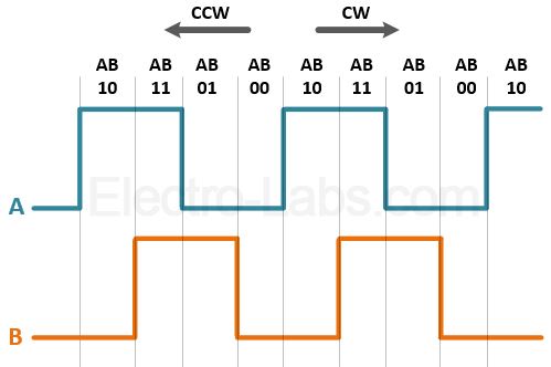
Rotary encoder signals (photo from:
electro-labs.com)
The encoder switches will produce less debouncing pulses when bypassed with 100nF capacitors:

Rotary encoder connection diagram
All pins of the encoder have internal pullup resistors. The basic idea is to trigger external interrupt EXTI with rising edge of the signal A. Within the EXTI interrupt service routine we will read the level of signal B and send message. Another external interrupt will be triggered by the pushbutton of the encoder. The rotary encoder shaft can be pushed down to close the key contact (marked with net name “Tipka-1” in the above schematic.
The encoder pinout is:
Signal A — PA10
Signal B — PA9
Key — PF0
STM32F0 External interrupt tutorial
I mentioned external interrupts. Let’s take a deeper look into the external interrupts. In order to trigger the EXTI ISR by transition on the external pin we will have to configure following blocks of the Cortex M0:
- Initialize GPIO pins
- Map EXTI line to GPIO pins
- Set EXTI triggers
- Unmask EXTI interrupt lines
- Assign EXTI interrupt priority
- Enable EXTI interrupts in nested interrupt vector controller (NVIC)
Let’s first define the pins:
//A - Pin for encoder "A" pin ---> triggers EXTI #define ENCODER_APORT GPIOA #define ENCODER_APINn 10 //B - Pin for encoder "B" pin #define ENCODER_BPORT GPIOA #define ENCODER_BPINn 9 //A - Pin for encoder "K" pin ---> KEy, triggers EXTI #define ENCODER_KPORT GPIOF #define ENCODER_KPINn 0 #define ENCODER_APIN ((uint16_t)(1U<<ENCODER_APINn)) #define ENCODER_BPIN ((uint16_t)(1U<<ENCODER_BPINn)) #define ENCODER_KPIN ((uint16_t)(1U<<ENCODER_KPINn)) |
Now we have to enable GPIO clock to enable GPIO configuration. Then we have to configure the pins as inputs with pullups. I will not repeat everything again. Please refer to the ADC section above for more details about GPIO configuration. All three GPIO pins are configured with:
/** Enable GPIO clocks for GPIOA and GPIOF */ RCC->AHBENR |= RCC_AHBENR_GPIOAEN; RCC->AHBENR |= RCC_AHBENR_GPIOFEN; /* Init GPIO Pins */ /* Encoder Pin A */ ENCODER_APORT->MODER &= ~(3ul << 2*ENCODER_APINn); ENCODER_APORT->OSPEEDR &= ~(3ul << 2*ENCODER_APINn); ENCODER_APORT->OSPEEDR |= (1ul << 2*ENCODER_APINn); ENCODER_APORT->PUPDR &= ~(3ul << 2*ENCODER_APINn); ENCODER_APORT->PUPDR |= (1ul << 2*ENCODER_APINn); /* Encoder Pin B */ ENCODER_BPORT->MODER &= ~(3ul << 2*ENCODER_BPINn); ENCODER_BPORT->OSPEEDR &= ~(3ul << 2*ENCODER_BPINn); ENCODER_BPORT->OSPEEDR |= (1ul << 2*ENCODER_BPINn); ENCODER_BPORT->PUPDR &= ~(3ul << 2*ENCODER_BPINn); ENCODER_BPORT->PUPDR |= (1ul << 2*ENCODER_BPINn); /* Encoder Key pin */ ENCODER_KPORT->MODER &= ~(3ul << 2*ENCODER_KPINn); ENCODER_KPORT->OSPEEDR &= ~(3ul << 2*ENCODER_KPINn); ENCODER_KPORT->OSPEEDR |= (1ul << 2*ENCODER_KPINn); ENCODER_KPORT->PUPDR &= ~(3ul << 2*ENCODER_KPINn); ENCODER_KPORT->PUPDR |= (1ul << 2*ENCODER_KPINn); |
In the Cortex M0 the external interrupt lines connection to the GPIOs are managed with the System configuration controller (SYSCFG). There are four SYSCFG external interrupt configuration registers: SYSCFG->EXTICR[0] to SYSCFG->EXTICR[3]. In each SYSCFG->EXTICR[n] register, there are four bits for each external interrupt line EXTI0 to EXTI15 selecting which pin is mapped to what EXTI line:
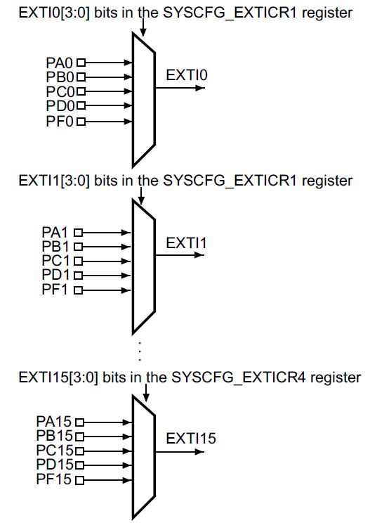
External interrupt/event GPIO mapping
The registers SYSCFG->EXTICR[0] to SYSCFG->EXTICR[3] have following structure (example for ):
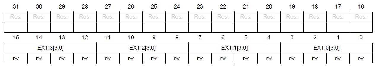
SYSCFG external interrupt configuration register1 SYSCFG->EXTICR[0]
x000: PA[x] pin
x001: PB[x] pin
x010: PC[x] pin
x011: PD[x] pin
x100: Reserved
x101: PF[x] pin
other configurations: reserved
Similar is register SYSCFG->EXTICR[1] for GPIO pins 4 to 7, SYSCFG->EXTICR[2] for GPIO pinf 8 to 11 and SYSCFG->EXTICR[3] for GPIO pins 12 to 15.
Don’t forget to enable clock for SYSCFG block before any configuration changes. Now we can map PA10 to GPIO External interrupt line 10 and PF0 to line 0:
/* Enable SYSCFG Clock */ RCC->APB2ENR |= RCC_APB2ENR_SYSCFGEN; /* Map EXTI10 line to PA10 */ SYSCFG->EXTICR[3] &= (uint16_t)~SYSCFG_EXTICR3_EXTI10_PA; SYSCFG->EXTICR[3] |= (uint16_t)SYSCFG_EXTICR3_EXTI10_PA; /* Map EXTI0 line to PF0 */ SYSCFG->EXTICR[0] &= (uint16_t)~SYSCFG_EXTICR1_EXTI0_PF; SYSCFG->EXTICR[0] |= (uint16_t)SYSCFG_EXTICR1_EXTI0_PF; |
Next step is to configure the Extended interrupts and events controller (EXTI).
In general, the extended interrupts and events controller (EXTI) manages the external and internal asynchronous events/interrupts and generates the event request to the CPU/Interrupt Controller and a wake-up request to the Power Manager. The EXTI allows the management of up to 28 external/internal event line (21 external event lines and 7 internal event lines).
For the external interrupt lines, to generate the interrupt, the interrupt line should be configured and enabled. This is done by programming the two trigger registers with the desired edge detection and by enabling the interrupt request by writing a ‘1’ to the corresponding bit in the interrupt mask register. When the selected edge occurs on the external interrupt line, an interrupt request is generated. The pending bit corresponding to the interrupt line is also set. This request is reset by writing a ‘1’ in the pending register. This is usually managed within the ISR.
Each line has one bit to enable rising edge trigger and one for falling edge trigger. When both are enabled, the EXTI line will trigger on both edges: rising and falling. In our case for encoder we need only one edge: falling (remember, we have pullups, the switch in the encoder connects pin to GND). EXTI lines 0 and 10 are configured to trigger on rising edge by writing 1 to corresponding bits in the EXTI->FTSR register:
/* EXTI0 line interrupts: set falling-edge trigger */ EXTI->FTSR |= EXTI_FTSR_TR0; /* EXTI0 line interrupts: clear rising-edge trigger */ EXTI->RTSR &= ~EXTI_RTSR_TR0; /* EXTI10 line interrupts: set falling-edge trigger */ EXTI->FTSR |= EXTI_FTSR_TR10; /* EXTI10 line interrupts: clear rising-edge trigger */ EXTI->RTSR &= ~EXTI_RTSR_TR10; |
The register EXTI->RTSR has reset value 0, but it doesnt hurt if we explicitly set the proper bits to 0 during setup. The register bit definitions are provided in the devide include file, so we can have more friendly and readable code.
The final step before enabling external interrupts is to unmask the EXTI lines. The Interrupt mask register EXTI->IMR has Bits 31:0 Interrupt mask on external/internal line x. Remeber: to unmask, the mask bit must be set to 1! Again we can use predefined symbols for unmasking the specific EXTI lines:
/* Unmask interrupts from EXTI0 line */ EXTI->IMR |= EXTI_IMR_MR0; /* Unmask interrupts from EXTI10 line */ EXTI->IMR |= EXTI_IMR_MR10; |
Now we can set the intreeupt priority and enable interrupts. The functions for handling the NVIC is provided by CMSIS Cortex-M0 Core Peripheral Access Layer. This is standardised for all Cortex-M0 microcontrollers. We have to spend few words about Nested vectored interrupt controller (NVIC). Not every EXTI line has own vector in the NVIC. For the Cortex M0, the EXTI lines are gathered into three groups. This means that several lines can trigger same interrupt. There are 32 interrupt channels in Cortex M0 and three channels are dedicated to EXTI triggers. Channel (or NVIC position) number 5 is for EXTI lines 0 and 1. The channel number 6 is for EXTI 2 and 3 and channel number 7 is for EXTI 4 to 15. The detailed description of NVIC programming is given in the Core peripherals chapter of PM0215 programming manual.
It is important to set Interrupt priority befor enabling the interrupt:
/* Assign EXTI interrupt priority = 2 in NVIC */ NVIC_SetPriority(EXTI4_15_IRQn, 2); NVIC_SetPriority(EXTI0_1_IRQn, 2); /* Enable EXTI interrupts in NVIC */ NVIC_EnableIRQ(EXTI4_15_IRQn); /** PA10 */ NVIC_EnableIRQ(EXTI0_1_IRQn); /** PF0 */ |
The GPIO external interrupt are finally concluded with proper Interrupt Service Routines. Here is the bare minimum, which don’t do anything except acknowledge the interrupts by clearing the interrupt pending flag. This is done by writing 1 to the flag in the EXTI pending register EXTI->PR:
// Encoder void EXTI4_15_IRQHandler(void) { if ((EXTI->PR & EXTI_PR_PR10) != 0) { // Clear EXTI interrupt pending flag (EXTI->PR). EXTI->PR |= EXTI_PR_PR10; } } // Key void EXTI0_1_IRQHandler(void) { if ((EXTI->PR & EXTI_PR_PR0) != 0) { // Clear EXTI interrupt pending flag (EXTI->PR). EXTI->PR |= EXTI_PR_PR0 ; } } |
User interface: 2×16 alphanumeric LCD
The final part is LCD to display readouts and provide access to the instrument settings.

2×16 Alphanumeric LCD
The LCD is connected to microcontroller with 6 signals. All signals are outputs at the microcontroller side. There is nothing dramatic about the 2×16 alphanumeric LCD. I took excellent library from Tilen Majerle and rewritten it to off-burden from HAL or any other libraries.
The pins are defined with same logic as already described above:
/// LCD pinout definitions //RS - Register select pin #define HD44780_RSPORT GPIOB #define HD44780_RSPINn 1 //E - Enable pin #define HD44780_EPORT GPIOA #define HD44780_EPINn 4 //D4 - Data 4 pin #define HD44780_D4PORT GPIOA #define HD44780_D4PINn 3 //D5 - Data 5 pin #define HD44780_D5PORT GPIOA #define HD44780_D5PINn 2 //D6 - Data 6 pin #define HD44780_D6PORT GPIOA #define HD44780_D6PINn 1 //D7 - Data 7 pin #define HD44780_D7PORT GPIOA #define HD44780_D7PINn 0 #define HD44780_RSPIN ((uint16_t)(1U<<HD44780_RSPINn)) #define HD44780_EPIN ((uint16_t)(1U<<HD44780_EPINn)) #define HD44780_D4PIN ((uint16_t)(1U<<HD44780_D4PINn)) #define HD44780_D5PIN ((uint16_t)(1U<<HD44780_D5PINn)) #define HD44780_D6PIN ((uint16_t)(1U<<HD44780_D6PINn)) #define HD44780_D7PIN ((uint16_t)(1U<<HD44780_D7PINn)) |
The pin handling is done with few macro definitions:
#define HD44780_RS_LOW HD44780_RSPORT->BSRR = HD44780_RSPIN<<16 #define HD44780_RS_HIGH HD44780_RSPORT->BSRR = HD44780_RSPIN #define HD44780_E_LOW HD44780_EPORT->BSRR = HD44780_EPIN<<16 #define HD44780_E_HIGH HD44780_EPORT->BSRR = HD44780_EPIN #define HD44780_E_BLINK HD44780_E_HIGH; HD44780_Delay(20); HD44780_E_LOW; HD44780_Delay(20) |
The LCD pins init procedure is:
static void HD44780_InitPins(void) { RCC->AHBENR |= RCC_AHBENR_GPIOAEN; /* Enable GPIOA clock */ RCC->AHBENR |= RCC_AHBENR_GPIOBEN; /* Enable GPIOB clock */ /* All pins push-pull, no pullup */ HD44780_RSPORT->MODER &= ~(3ul << 2*HD44780_RSPINn); HD44780_RSPORT->MODER |= (1ul << 2*HD44780_RSPINn); HD44780_RSPORT->OTYPER &= ~(1ul << HD44780_RSPINn); HD44780_RSPORT->OSPEEDR &= ~(3ul << 2*HD44780_RSPINn); HD44780_RSPORT->OSPEEDR |= (1ul << 2*HD44780_RSPINn); HD44780_RSPORT->PUPDR &= ~(3ul << 2*HD44780_RSPINn); HD44780_EPORT->MODER &= ~(3ul << 2*HD44780_EPINn); HD44780_EPORT->MODER |= (1ul << 2*HD44780_EPINn); HD44780_EPORT->OTYPER &= ~(1ul << HD44780_EPINn); HD44780_EPORT->OSPEEDR &= ~(3ul << 2*HD44780_EPINn); HD44780_EPORT->OSPEEDR |= (1ul << 2*HD44780_EPINn); HD44780_EPORT->PUPDR &= ~(3ul << 2*HD44780_EPINn); HD44780_D4PORT->MODER &= ~(3ul << 2*HD44780_D4PINn); HD44780_D4PORT->MODER |= (1ul << 2*HD44780_D4PINn); HD44780_D4PORT->OTYPER &= ~(1ul << HD44780_D4PINn); HD44780_D4PORT->OSPEEDR &= ~(3ul << 2*HD44780_D4PINn); HD44780_D4PORT->OSPEEDR |= (1ul << 2*HD44780_D4PINn); HD44780_D4PORT->PUPDR &= ~(3ul << 2*HD44780_D4PINn); HD44780_D5PORT->MODER &= ~(3ul << 2*HD44780_D5PINn); HD44780_D5PORT->MODER |= (1ul << 2*HD44780_D5PINn); HD44780_D5PORT->OTYPER &= ~(1ul << HD44780_D5PINn); HD44780_D5PORT->OSPEEDR &= ~(3ul << 2*HD44780_D5PINn); HD44780_D5PORT->OSPEEDR |= (1ul << 2*HD44780_D5PINn); HD44780_D5PORT->PUPDR &= ~(3ul << 2*HD44780_D5PINn); HD44780_D6PORT->MODER &= ~(3ul << 2*HD44780_D6PINn); HD44780_D6PORT->MODER |= (1ul << 2*HD44780_D6PINn); HD44780_D6PORT->OTYPER &= ~(1ul << HD44780_D6PINn); HD44780_D6PORT->OSPEEDR &= ~(3ul << 2*HD44780_D6PINn); HD44780_D6PORT->OSPEEDR |= (1ul << 2*HD44780_D6PINn); HD44780_D6PORT->PUPDR &= ~(3ul << 2*HD44780_D6PINn); HD44780_D7PORT->MODER &= ~(3ul << 2*HD44780_D7PINn); HD44780_D7PORT->MODER |= (1ul << 2*HD44780_D7PINn); HD44780_D7PORT->OTYPER &= ~(1ul << HD44780_D7PINn); HD44780_D7PORT->OSPEEDR &= ~(3ul << 2*HD44780_D7PINn); HD44780_D7PORT->OSPEEDR |= (1ul << 2*HD44780_D7PINn); HD44780_D7PORT->PUPDR &= ~(3ul << 2*HD44780_D7PINn); } |
Function to send data via 4 bit interface:
static void HD44780_Cmd4bit(uint8_t cmd) { /* Set output port */ HD44780_D7PORT->BSRR = HD44780_D7PIN<<((cmd & 0x08) ? 0 : 16); HD44780_D6PORT->BSRR = HD44780_D6PIN<<((cmd & 0x04) ? 0 : 16); HD44780_D5PORT->BSRR = HD44780_D5PIN<<((cmd & 0x02) ? 0 : 16); HD44780_D4PORT->BSRR = HD44780_D4PIN<<((cmd & 0x01) ? 0 : 16); HD44780_E_BLINK; } The simple microsecond delay function is: |
static void HD44780_Delay(uint32_t us) { us *= 48; while (us--) __nop(); } |
And finally, the LCD init and clear:
void HD44780_Init(uint8_t cols, uint8_t rows) { /* Init pinout */ HD44780_InitPins(); /* At least 40ms */ osDelay(45); /* Set LCD width and height */ HD44780_Opts.Rows = rows; HD44780_Opts.Cols = cols; /* Set cursor pointer to beginning for LCD */ HD44780_Opts.currentX = 0; HD44780_Opts.currentY = 0; HD44780_Opts.DisplayFunction = HD44780_4BITMODE | HD44780_5x8DOTS | HD44780_1LINE; if (rows > 1) { HD44780_Opts.DisplayFunction |= HD44780_2LINE; } /* Try to set 4bit mode */ HD44780_Cmd4bit(0x03); osDelay(5); /* Second try */ HD44780_Cmd4bit(0x03); osDelay(5); /* Third goo! */ HD44780_Cmd4bit(0x03); osDelay(5); /* Set 4-bit interface */ HD44780_Cmd4bit(0x02); osDelay(1); /* Set # lines, font size, etc. */ HD44780_Cmd(HD44780_FUNCTIONSET | HD44780_Opts.DisplayFunction); /* Turn the display on with no cursor or blinking default */ HD44780_Opts.DisplayControl = HD44780_DISPLAYON; HD44780_DisplayOn(); /* Clear lcd */ HD44780_Clear(); /* Default font directions */ HD44780_Opts.DisplayMode = HD44780_ENTRYLEFT | HD44780_ENTRYSHIFTDECREMENT; HD44780_Cmd(HD44780_ENTRYMODESET | HD44780_Opts.DisplayMode); /* Delay */ osDelay(5); } void HD44780_Clear(void) { HD44780_Cmd(HD44780_CLEARDISPLAY); //HD44780_Delay(3000); osDelay(3); } |
Complete source code is available in GitHub repository s54mtb/pHmeter.