Altium – working with embedded boards
Embedded board arrays in altium could be used for creating panels for multiplication during prototyping. Here is short illustrative example. In this example we will:
- create single PCB board design (not covered here)
- create and embed array with this single PCB
- add some markers and holes
- add panel cutouts

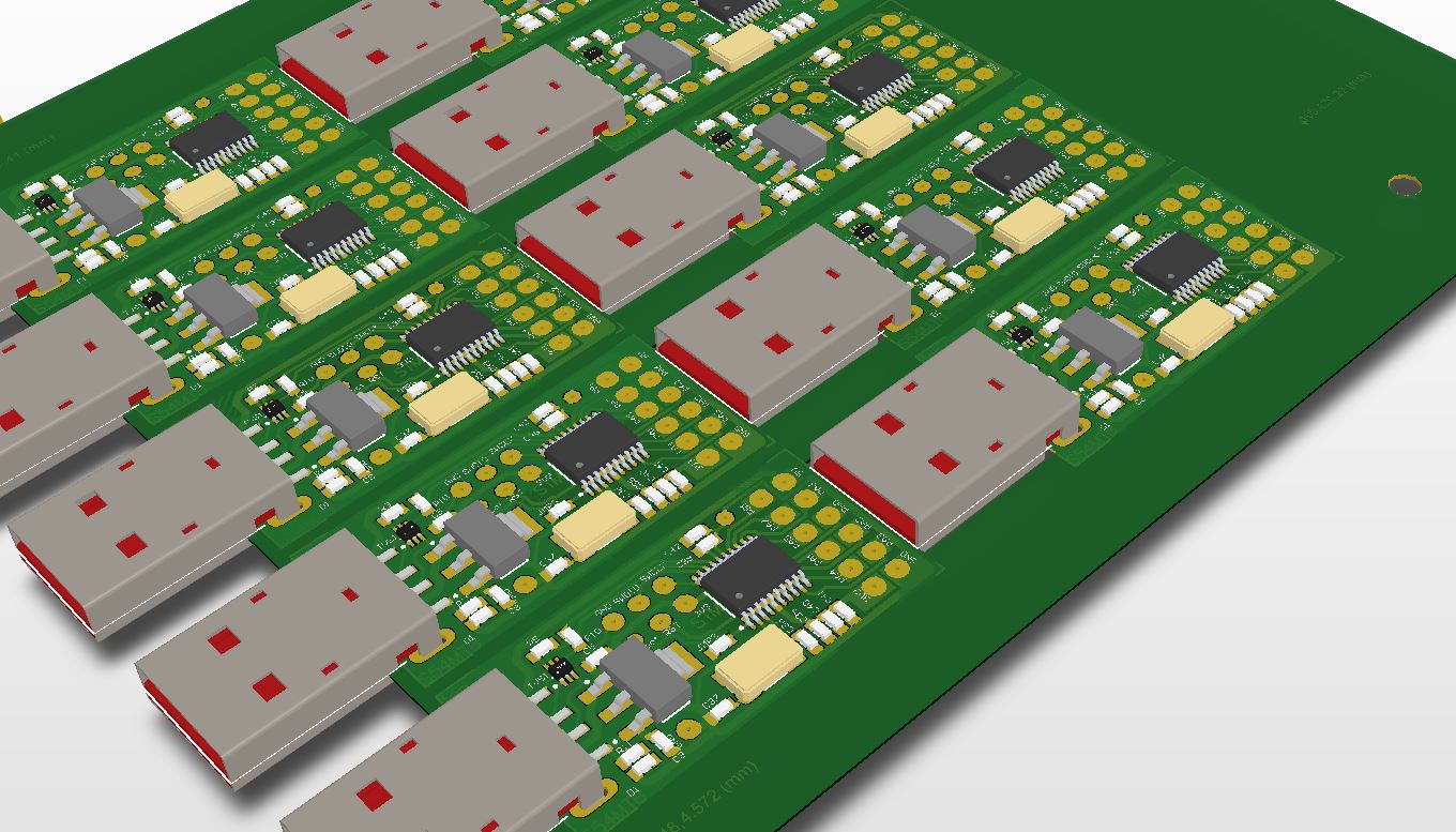
Final result, keep reading below…
First you have to design your single PCB.
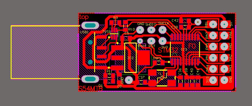
Single PCB design
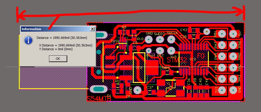
Measure and remember the outline dimensions of the board (R,B or Ctrl-M):
Next add new blank PCB to the project. Insert embedded board using your single PCB design and dimensions. Enter number of rows and columns. In our case we would like to produce 10 boards:
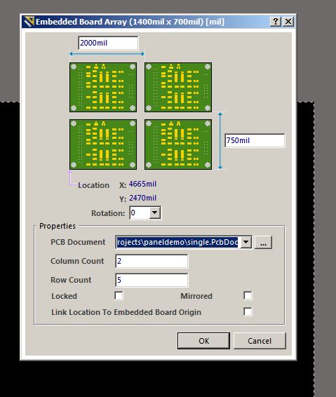
Insert embedded board
Place it anywhere on the working area and draw the outline using keepout layer around the array.
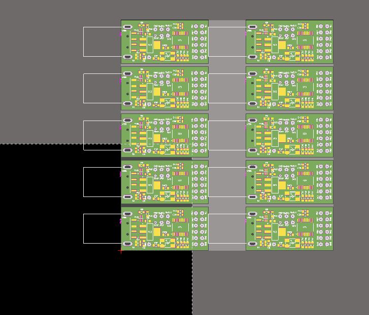
Embedded array is placed “somewhere”
Keep in mind that board shape from single boards will be overriden by panel board. Execute usual commands E,S,Y and D,S,D to define new board shape from drawn lines in keepout layer.
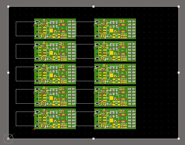
Define shape of panel PCB
Now add PADS for holes in panel, coordinate markers and any other features you may want to see on the panel border. You can even add custom cutouts in the panel: just draw closed shapes and use command Tools-Convert-Create board cutout from selected objects (T,V,T):
In our example cutouts are for USB connectors in case we assemble the PCBs in the panel.
If you have any questions, please post them below as comments. I will answer ASAP.